Ergodox Aleph Build Log Chapter 2: Building A Board
crossposted from cohost
The first thing any good project needs is a name. I certainly couldn't call it the Ergodox Infinity 2. For one, it was hardly an authorised sequel. I've spoken to the original board designer a few times on Discord, so it's not a complete vacuum, but certainly I don't plan on sending a pull request when I'm done.
For another, you can't have infinity times two. That doesn't make any sense. If you need bigger infinities, you use Aleph numbers.
(Please don't ask me what that means. I'm many things but none of them are “math understander”).
Midway through the design process I had a brief crisis of faith - was it just ego, giving my board a new name to a mostly-rehashed product? I talked to a number of people in some Keyboard discords, and they assured me that “adding addressable RGB LEDs” is more than enough difference to justify my moniker.
The Ergodox Aleph was a go.
Circuit Boards
I've been curious about building my own circuit boards for a while now. When I lived in Toronto, I was a member of a hackerspace where it seemed like everyone was putting in Digikey orders, and the space was covered with purple OSHPark boards. At that point I barely knew how to solder, and was also trying to finish a degree in computer science, so I never got the chance to try. Now one had landed in my lap
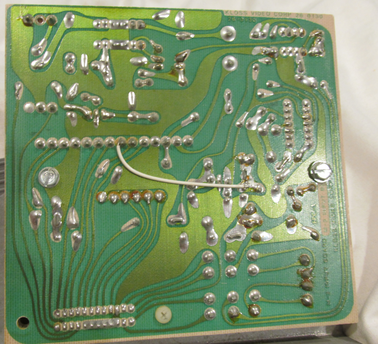
In theory, you can build a circuit board mostly by hand, and that's how it was done in days of yore. You buy a piece of fibreglass covered in copper, mask it with something like a sharpie, and etch it. “Etch” could mean physically, and some people do actually build simple PCBs with CNC routers. But usually it involves a bunch of unpleasant chemicals and an extremely well ventilated space. These produce beautiful, almost organic-looking circuit boards.
EDA Basics
Modern boards, like almost anything modern, are no longer made by hand. Instead, you design your board in a specialised piece of software called an (TODO) EDA. At my old hackerspace EAGLE (now owned by Autodesk) was the tool of choice. But just as popular is an entirely open-source tool called KiCAD.
Luckily for me, the Ergodox Infinity was built with KiCAD, so I didn't need to “acquire” EAGLE or deal with importing. I could get straight to work.
This is not a tutorial! I barely know what I'm doing, and there's many more excellent KiCAD and EDA resources available on the online. I got a ton of advice from hadi's youtube series.
EDAs are usually used in two steps. First, you lay out a circuit diagram symbolically in a schematic.
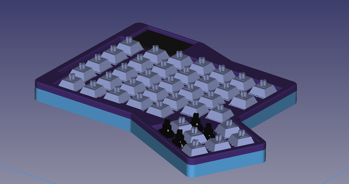
This was mostly done for me, but I wanted to add LEDs, so I built out a sample circuit for those two.
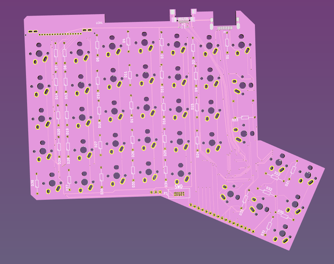
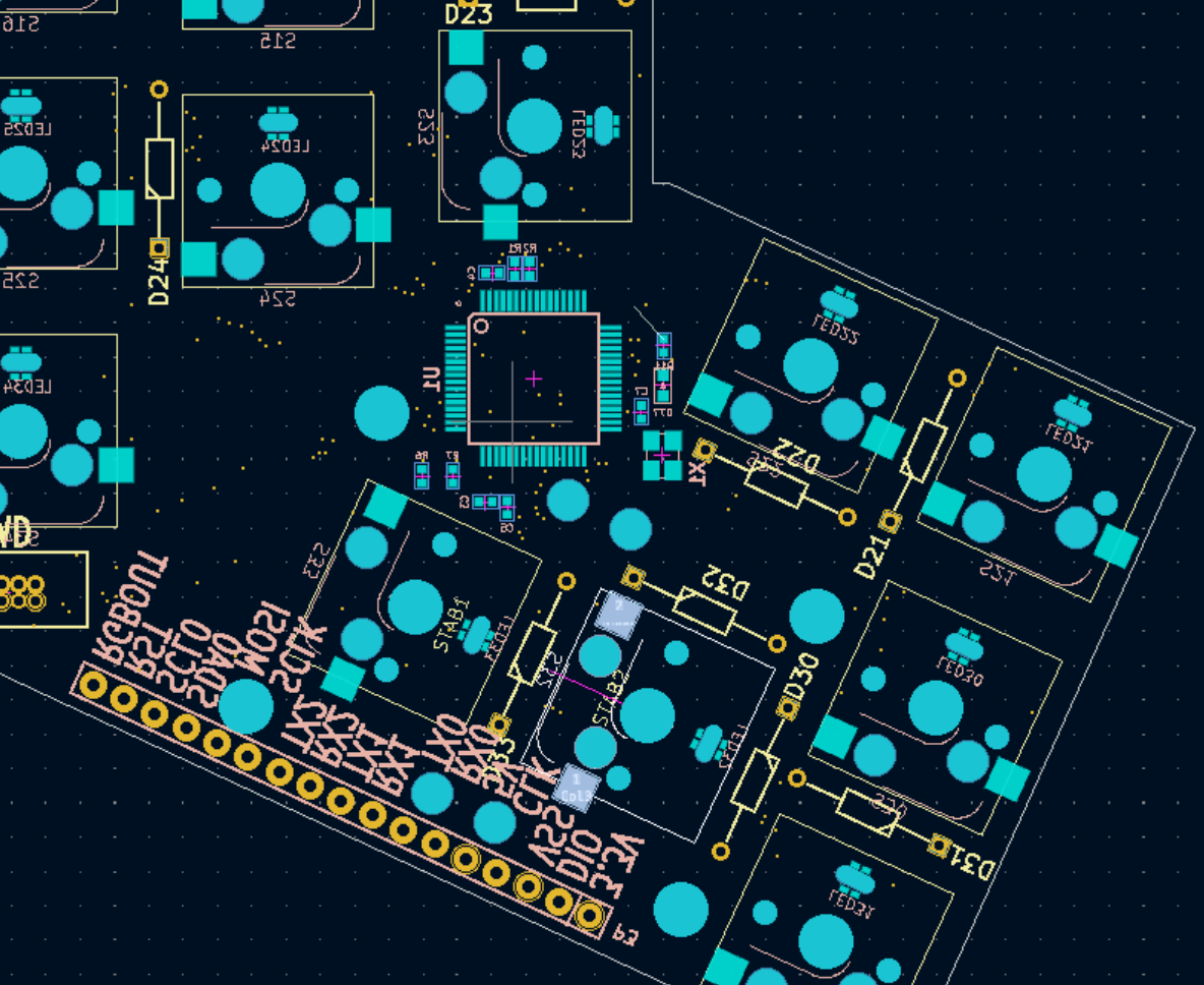
Then, you switch to the PCB Editor. You lay out all your components, which was again mostly already done. But I had to carefully align my LEDs such that they fell directly under the keyboard footprints.
Then, it's time for either the best or the worst part. You've just arranged your components on the board, but they're not connected to each other.
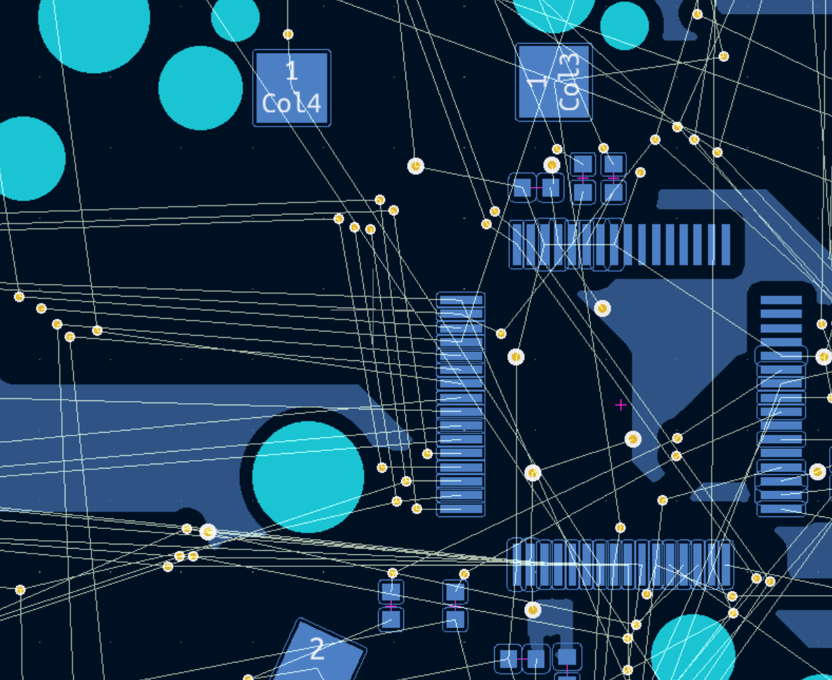
Each component has one or more “pads,” and “ surfaces that components will eventually be soldered to the board. The EDA will tell you which pads need
It's up to you to solve this several-hundred-utilities problem. Your tools? You can draw traces, and drill holes. Traces can be on either side of the board, and holes connect one side to the other.
This can be a sort of zen experience, a puzzle game with a purpose. Broadly speaking, I try to put horizontal lines on one side and vertical on the other, which reduces conflicts. But they certainly aren't eliminated. KiCad has a little counter in the bottom with how many unrouted lines you've got, and I spent two days bringing that number down to zero.
All of the components already on the board were connected already, but I ended up needing to rip most of them up.
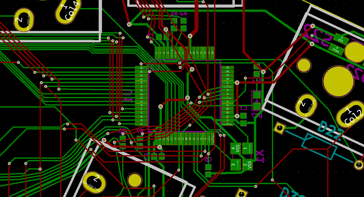
It gets harder as you go, too. The more lines you connect, the more board space you've taken up, and the less space there is for new traces. High-performance circuit boards like a modern motherboard have many more than the front-and-back layers I have access to, but those are much more expensive to produce. It's definitely half art half skill. And some of the results are extremely satisfying.
Board Clearances
After giving the board a very careful once, twice, thrice-over, I was just about ready to send it off to be manufactured. I used my friend sen's final checklist, then I exported the files my chosen fabricator needed, hit upload, and sat back to wait.
Fortunately, I got an email back almost immediately. Unfortunately, it was not good news..
As shown below, some hole to trace clearance, slots to trace clearance is too narrow.
So some trace might be cut. And there is no space to move the trace.
Is that OK if proceed per gerber?
Or shall we cancel it for you to replace file?
You see, there's a very important settings menu in KiCAD I'd neglected to check. Not every PCB manufacturer has the exact same manufacturing capabilities, so it's important to check their specifications page, and set up the design constraints accordingly.
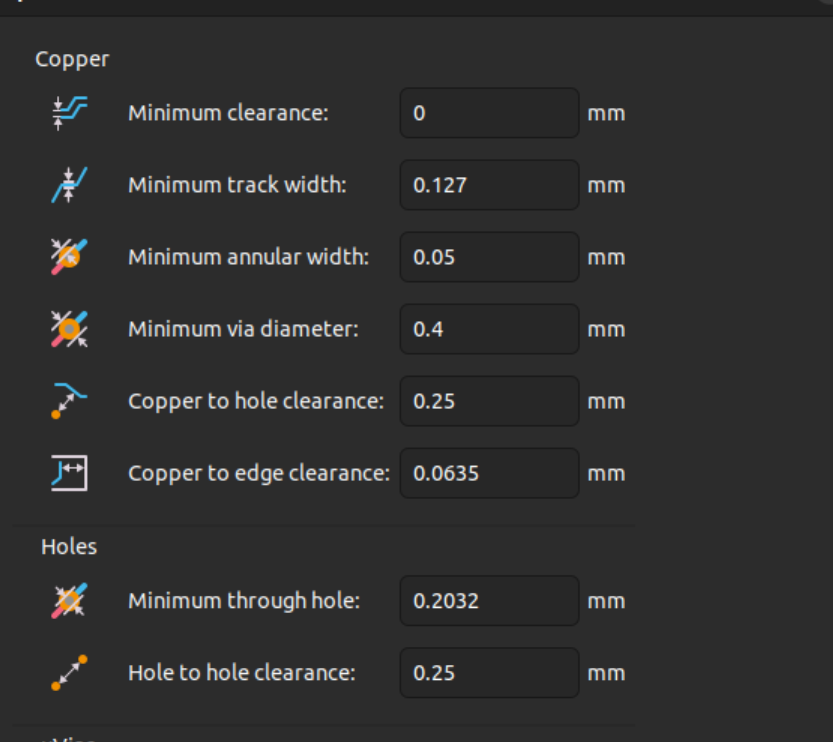
I had not done this. And because I hadn't done this, all my traces were to close to holes, and they might get cut off. All these companies, even the very cheap ones I was using, use semi-automated, semi-manual checks to make sure a board can be manufactured. Mine might work, but it also might just be missing critical pieces.
And of course, since I'd designed my boards wrong from the start, I had unacceptably small tolerances all over the board. But that was okay, because I wanted to make another change.
LEDs
When you think of addressable RGBs, you might think of Adafruit Neopixels or any number of clones. Those strips are mostly based on a specific component called "WS2812B,” which really rolls of the tongue.
These are a bit of a clever piece of kit. LEDs themselves are not very smart, they can just turn on and off. But these have a little chip inside them, one that makes them a little smarter. In essence, you can wire up a long chain of them and they will all talk to each other. You simply wire their data pins together in series, and like a bucket brigade they pass signals down the chain.
I decided I didn't want to do this. I was worried about power consumption - those built in chips didn't use much power, but they did have some constant current draw, even when the LEDs themselves were off.
I also didn't really understand how to calculate duty cycles, so I didn't know how many LEDs would be on at any given time.
Instead, I decided to use a dedicated LED controller chip. This would allow me to use cheaper dumb LEDs, and it would give me centralised control over them. Lower power consumption overall, good control.
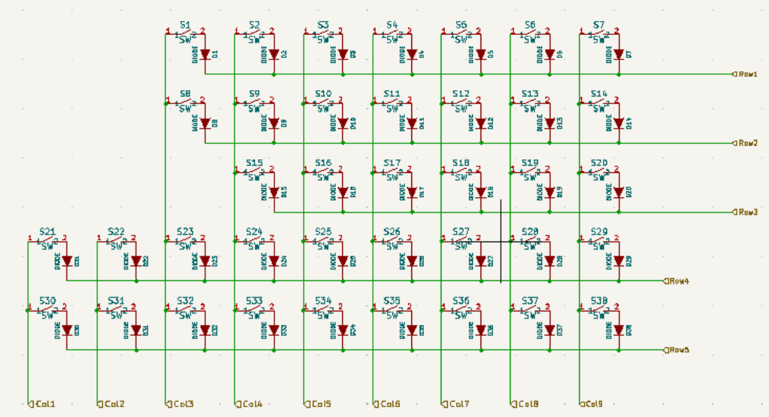
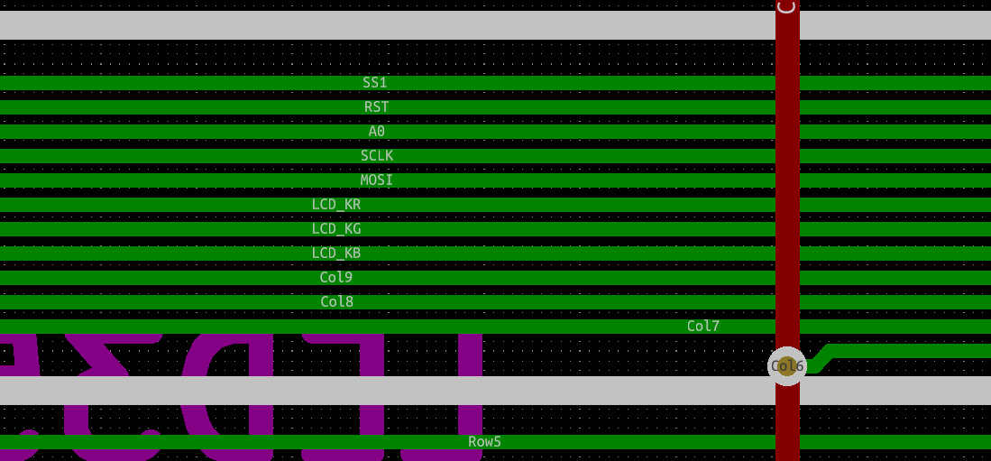
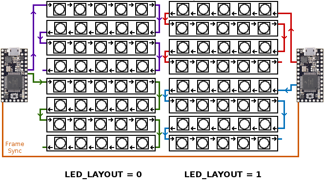
There's just one problem: Because the LEDs aren't smart, you need to wire every single one back to the controller. Three times, one for each of Red, Green, and Blue. They form a matrix, and in software you write “row 6 column 5 turn on,” and the LED at that intersection turns on.
This is an insane thing to do.
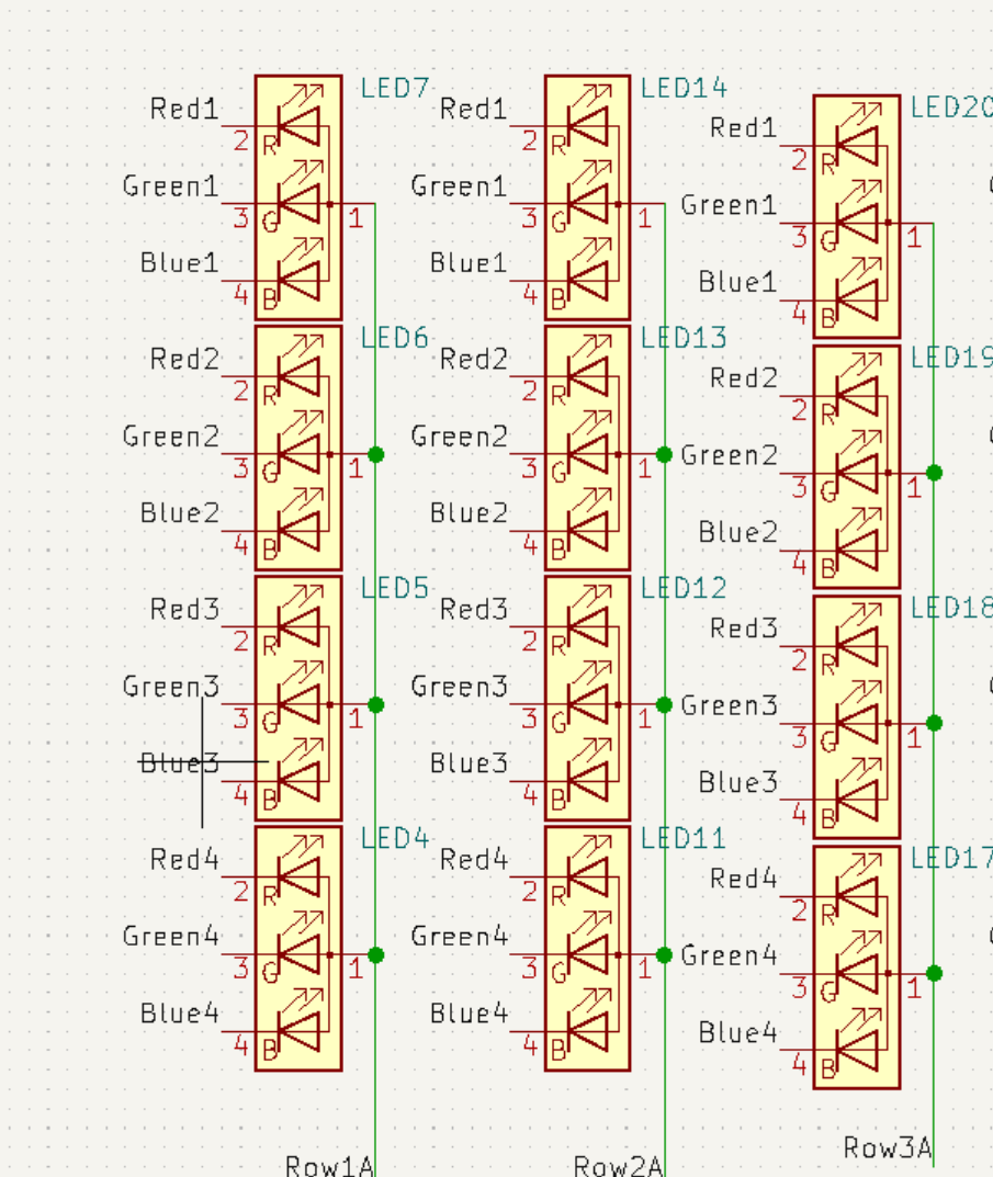
But I did it anyway.
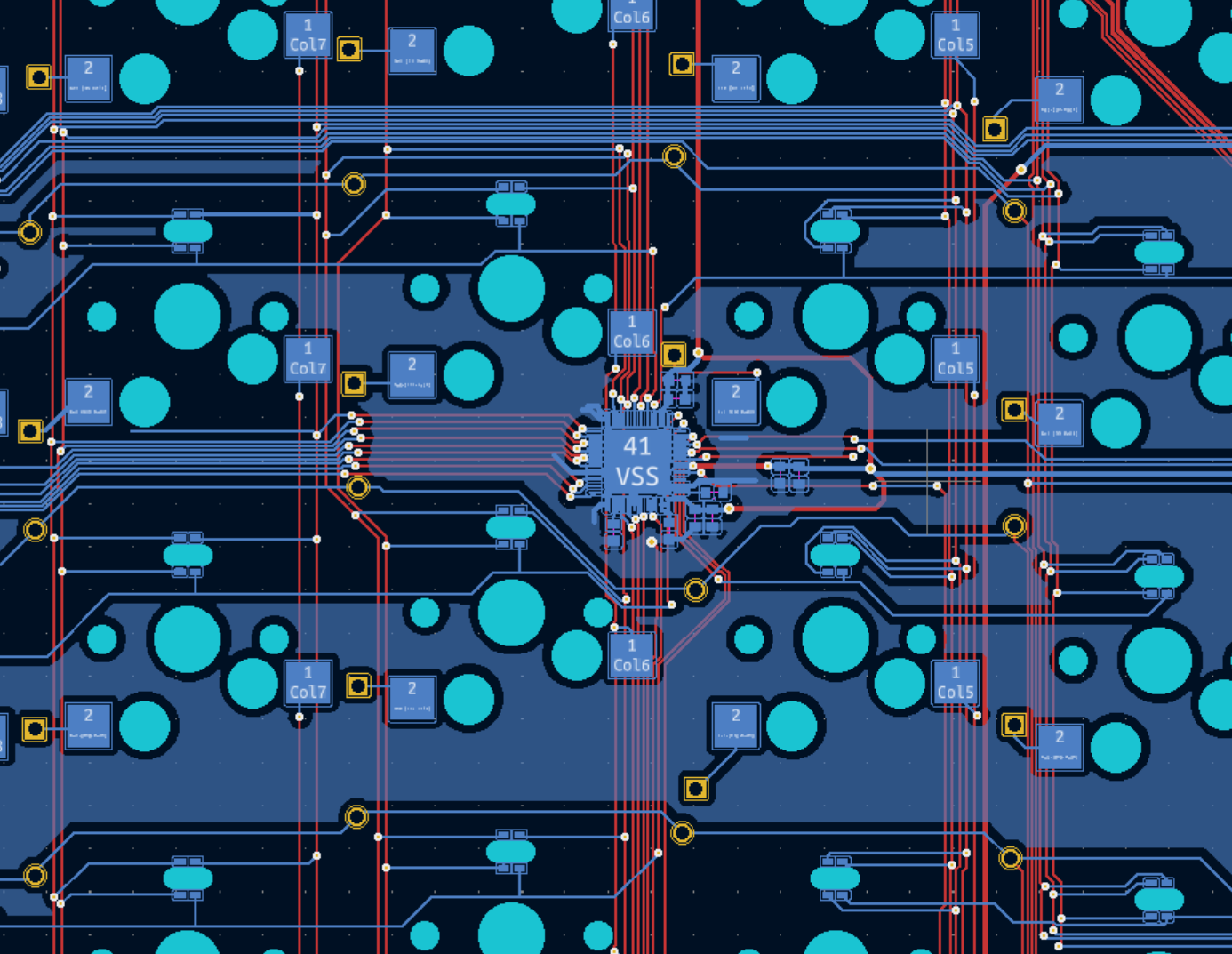
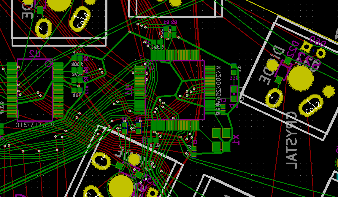
It took me many more days to route, but I eventually got into a groove, and I routed the entire board.
Conclusion
I ended up making another couple changes. I added holes for stabilisers, added my hot-swap switches, and switched out the tiny surface diodes for big through-hole ones I hope would be easier to install.
But after a few days, there was no more procrastination. I sent my board back to the fabricators, it passed QA, and then it was time to wait.
But I didn't just twiddle my thumbs.
Next time on the aleph build log: we make a case.