Ergodox Aleph Build Log Chapter 4: Soldering On
crossposted from cohost
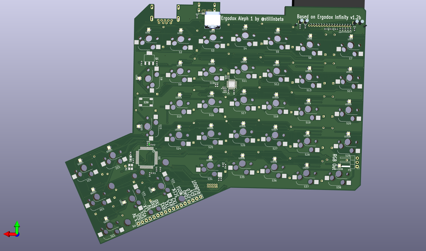
The boards came!
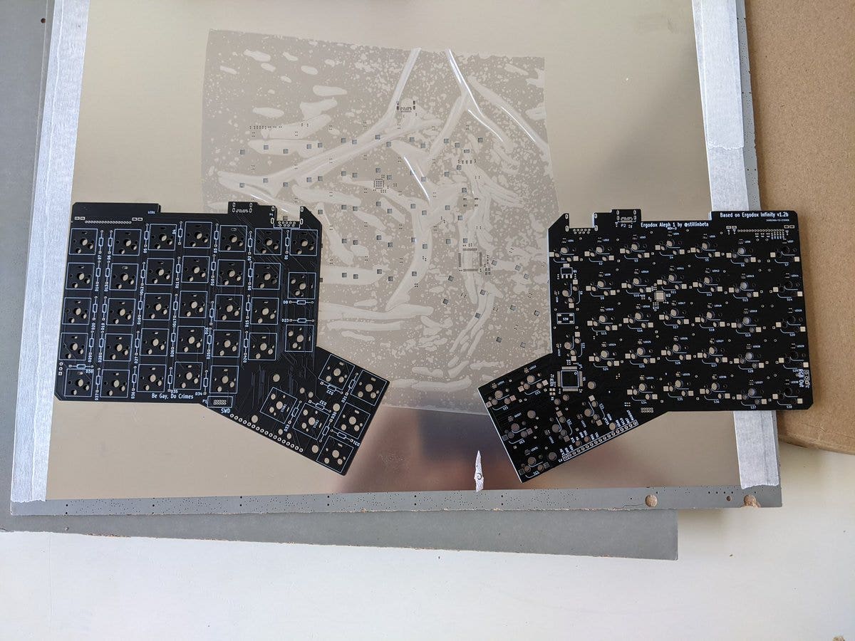
Now it's time to solder.
When you think of soldering, if you think of anything at all, you probably think of what is now called “through-hole.” A component has long leads, they go through holes drilled in the board, leads get soldered then trimmed.
This can be automated on an industrial scale, but it's expensive and time consuming. Instead, almost all modern microelectronics is done with surface-mount components. As the name suggests, these components are soldered only to the top of the board - no holes to drill, leads to trim, or voids to fill.
Introduction to Surface-mount Devices
Surface-mount soldering is usually accomplished by using Solder Paste, an incredibly expensive combination of solder and flux paste. The flux serves to hold components in place, while the solder serves to attach them when heated up. Then when heat is applied, the flux melts away and the solder attaches components firmly to the pads.
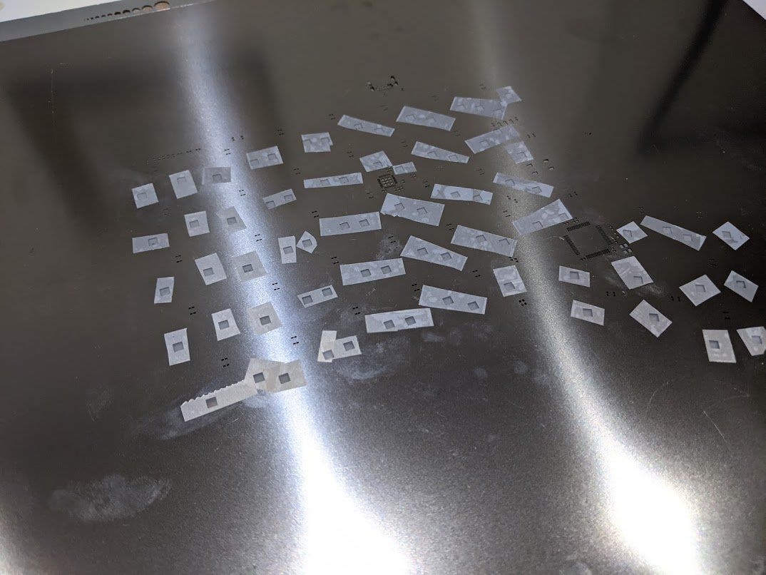
One board can have hundreds of components on even more pads, so the point-by-point application of paste is cumbersome and inefficient. Instead, most assembly houses will use a “solder mask,” literally a thin piece of metal with holes cut out where the pads are. That way, you can just squeegee on exactly as much paste as you need, and it will all go in the right spots.
The board manufacturing house I picked will sell you a solder mask to go with your board for a small extra fee. I didn't intend to build a lot, but I thought the solder mask would make assembly for the few I did easier.
Kailh Hot-swap Sockets
You might notice there's some pieces of tape on that solder mask. It did not come that way! But take a look at the back of the board. Those large squares are intended to hold Kailh Hot-swap Sockets:
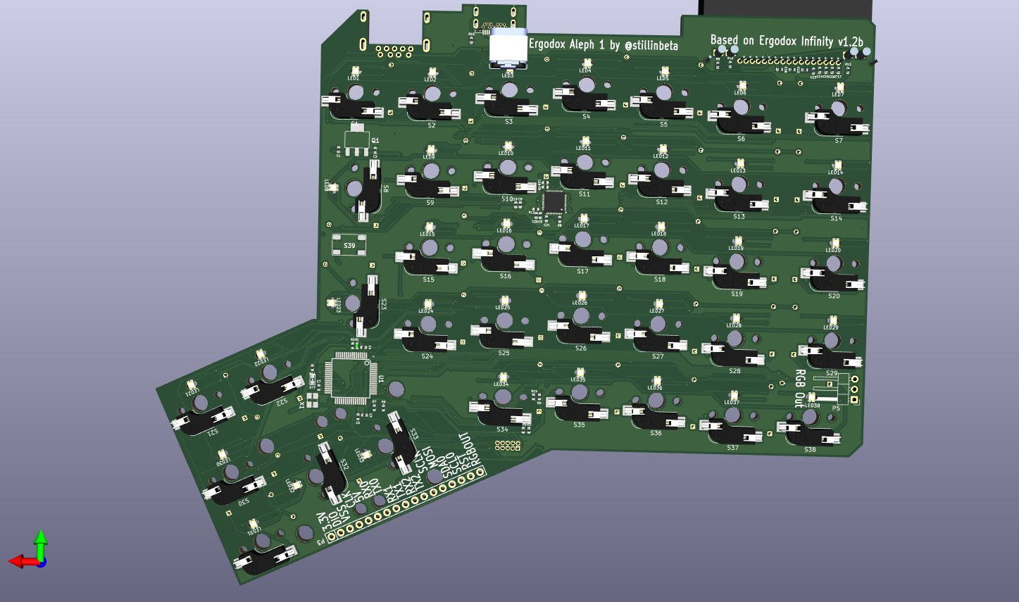
Now, these are technically surface-mount components. But I was advised that solder paste connections may not be mechanically sturdy enough to stand up to repeated replacements of keyswitches. They would also require a lot of solder paste, and as I mentioned earlier, it's very expensive. So I elected to tape over those holes. Once everything was assembled, I would go through and hand-solder them with the through-hole diodes I selected.
If you're very observant, you might see the solder mask in the picture is backwards from the images of the board I posted. Is this some clever geometry play? No. After I took this picture I realised I'd taped the wrong side, and had to rip it up and start over.
Pick-and-Place
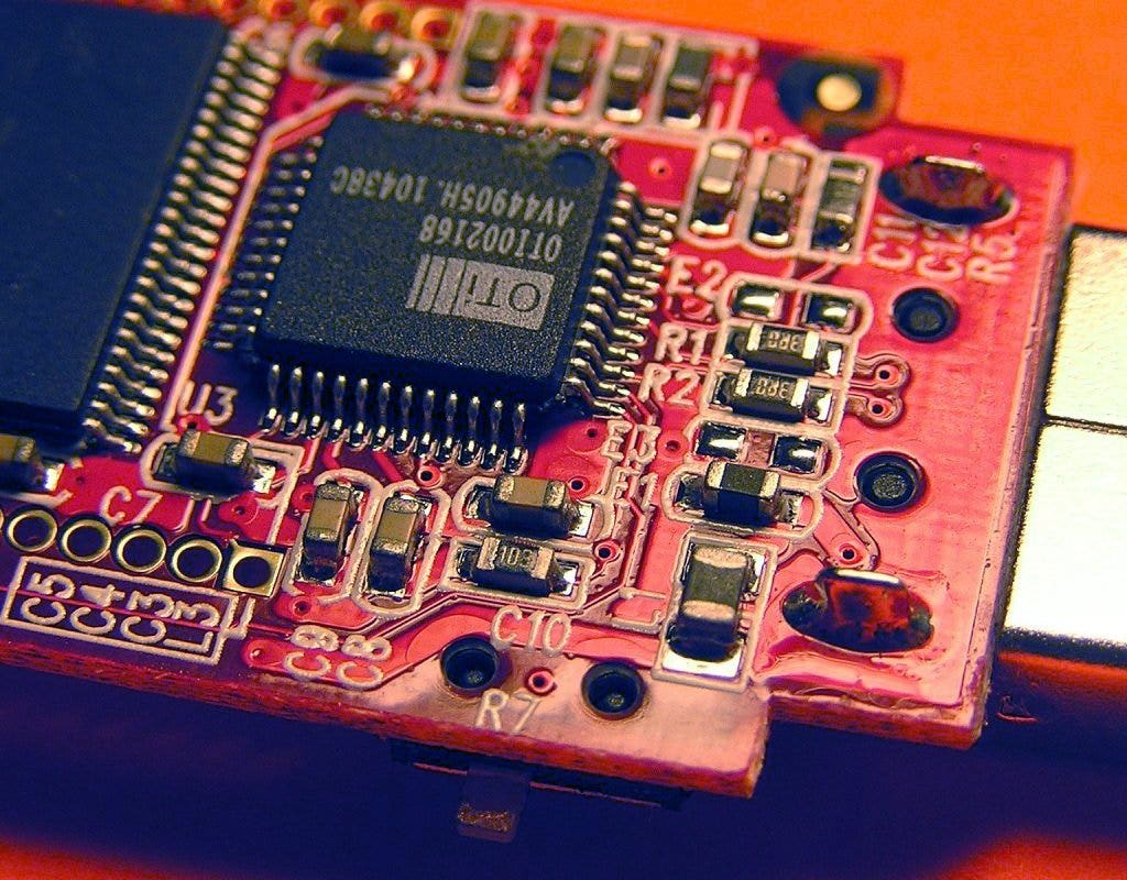
After the solder mask goes on, all the tiny little SMD components have to be physically placed on the board, a process called “population.” Professional board houses use automated tools called “pick-and-place machines” to place all the individual components on the board in the right places. These are mesmerising, extremely accurate, and cost (on the absolute lowest hobby-grade end) several thousand dollars.
So instead, I used this Pick-and-place:

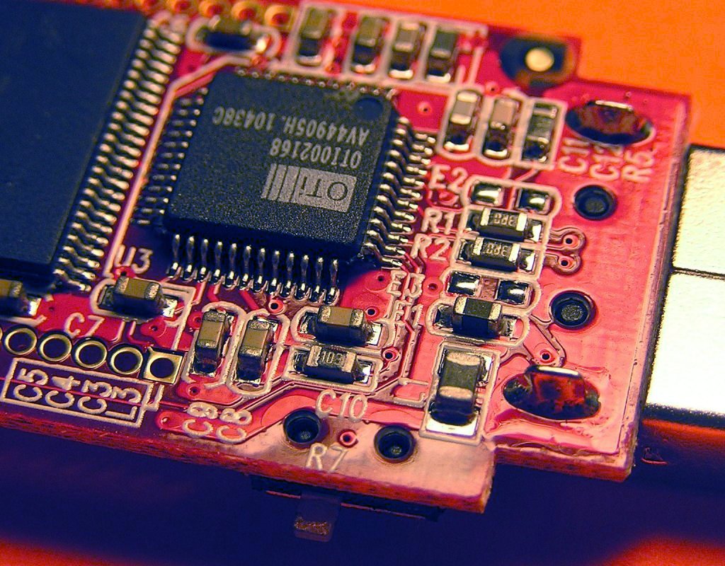
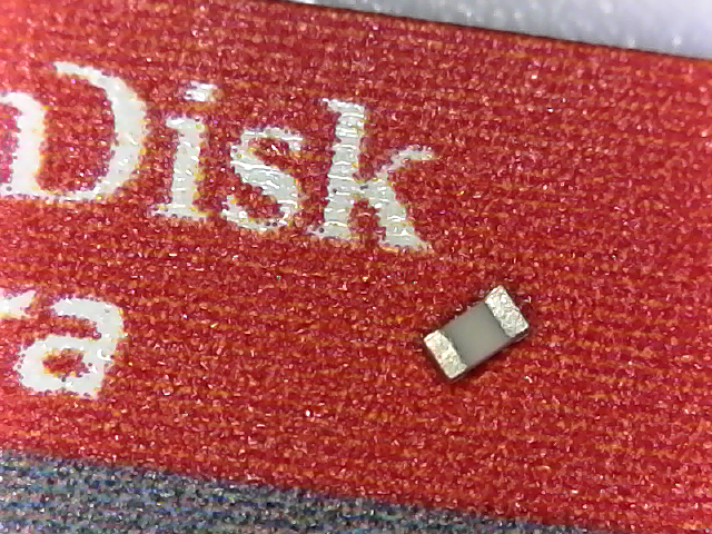
It's a time-consuming, extremely fiddly process to populate all of these boards. It is also the time when you realise that it's all well and good to pick a 1005 diode in your extremely zoomed-in IDE, but 1.0x0.5mm is very, very small, and this will not be an easy process.
The components mostly come in paper tape, intended for the less organic pick and place machines. To make assembly easier, I placed pieces of tape in these small boxes Adafruit sells for this purpose. At one point I tried removing some of the passive components from their tape and placing them loose in the boxes. Do not do this, you will never see half of those objects again.
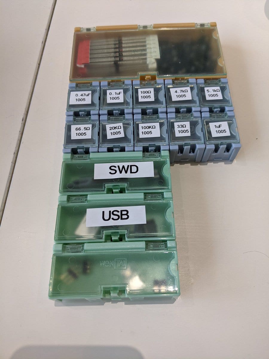
It took me a while to get into a rhythm. I made a spreadsheet that listed the component numbers by part type, so I could first populate “every 33Ω resistor,” then “every 5.6kΩ resistor,” etc. It is important to go carefully and in order - these components are too small to have labels. Several times I dropped a component on my assembly mat, and because I wasn't sure which one it was I just had to discard it. Diodes are directional too - they have a tiny white spot that lines up (hopefully) with the dot on the PCB.
There's also some time pressure here - as soon as you get the solder paste applies it starts to dessicate. I would set aside an evening to do the whole process, from applying solder paste to populating to reflow.
Reflow
“Reflow” is the process of melting the flux the solder paste is suspended in, liquifying the solder and bonding components to the PCB. There are two primary ways to do this.
The classic and commercial way is in an oven. You slowly and carefully raise the entire board to a given temperature, leave it there just long enough to melt the solder, then cool it again. There are commercial ovens that do this, but hobbyists often repurpose old toaster ovens.
I elected to go the other main route: I bought a Chinese hot air rework station off Ebay. These are usually intended for doing repairs, but for small-scale board assembly like I was doing they would (hopefully) work just fine.
Once I got everything populated and double-checked, I set up the hot air station and started from the top right, working my way down. Sometimes I got the fan a little too high and I blew some diodes straight off the board. I was constantly tweaking the temperature settings - it wasn't clear to me how the hot air temperature corresponded with contact-soldering temperatures. Also, the project mat I was doing wasn't as heat-resistant as I thought and I badly warped it.
But after about an hour of frustrating work, I finally had one properly assembled, beautiful-looking board.
No you didn't.
If only it were that easy. Instead, I found things like this:
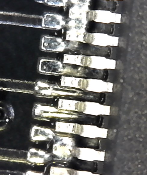
I've seen tons of videos of almost magical SMD assembly - a combination of surface tension and heat that seats chips with dozens of pins perfectly every time. But the instructions were very much of the “draw the rest of the owl.”
I ended up doing a bunch of trial-and-error work. I used a combination of desoldering wick, a soldering iron, flux, rubbing alcohol, and more solder paste.
In retrospect I was probably storing my solder paste improperly (I keep it in the fridge now.) But after a lot of trial and error, and melting one of the SWD connectors I got everything mostly working. I even managed to connect my Segger J-Link to the chip and program it. Excited, I flashed an image of QMK, hoping to see the RGB blinkenlights I'd spent so much time routing.
They did not blinken.
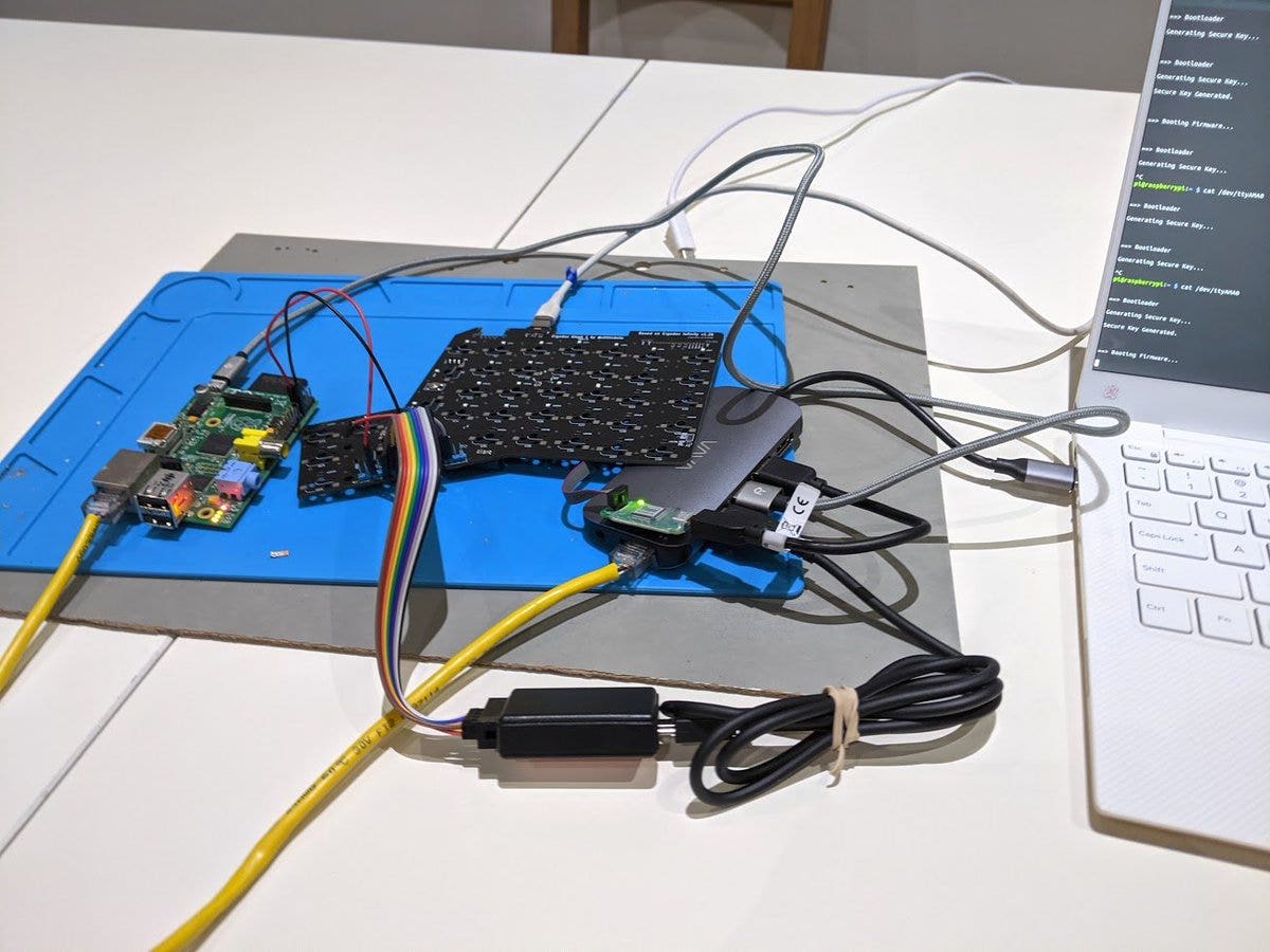
Next time on Aleph Build Log: One of Ten Thousand Things Is Wrong And I Have To Figure Out What